The $10 Billion Question Everyone’s Asking
When
NVIDIA announced its Blackwell architecture in March 2024, the AI industry held its breath. Promising 30x performance improvements over Hopper for AI inference and 4x faster training, the B100 and B200 GPUs weren’t just incremental upgrades they represented a fundamental leap in AI computing capability.But by August 2024, whispers turned into headlines: Blackwell was delayed. Not by weeks, but by months. Major customers like Microsoft, Google, Meta, and Amazon who had collectively placed orders worth tens of billions of dollars faced the prospect of waiting until 2025 for their AI infrastructure.
What actually went wrong? And more importantly, why did NVIDIA CEO Jensen Huang take the unusual step of publicly declaring the design flaw was “100% NVIDIA’s fault”?
This isn’t just a story about delayed silicon. It’s a case study in the brutal complexity of modern AI hardware, the challenges of pushing manufacturing limits, and why sometimes slowing down is the only way to move forward.
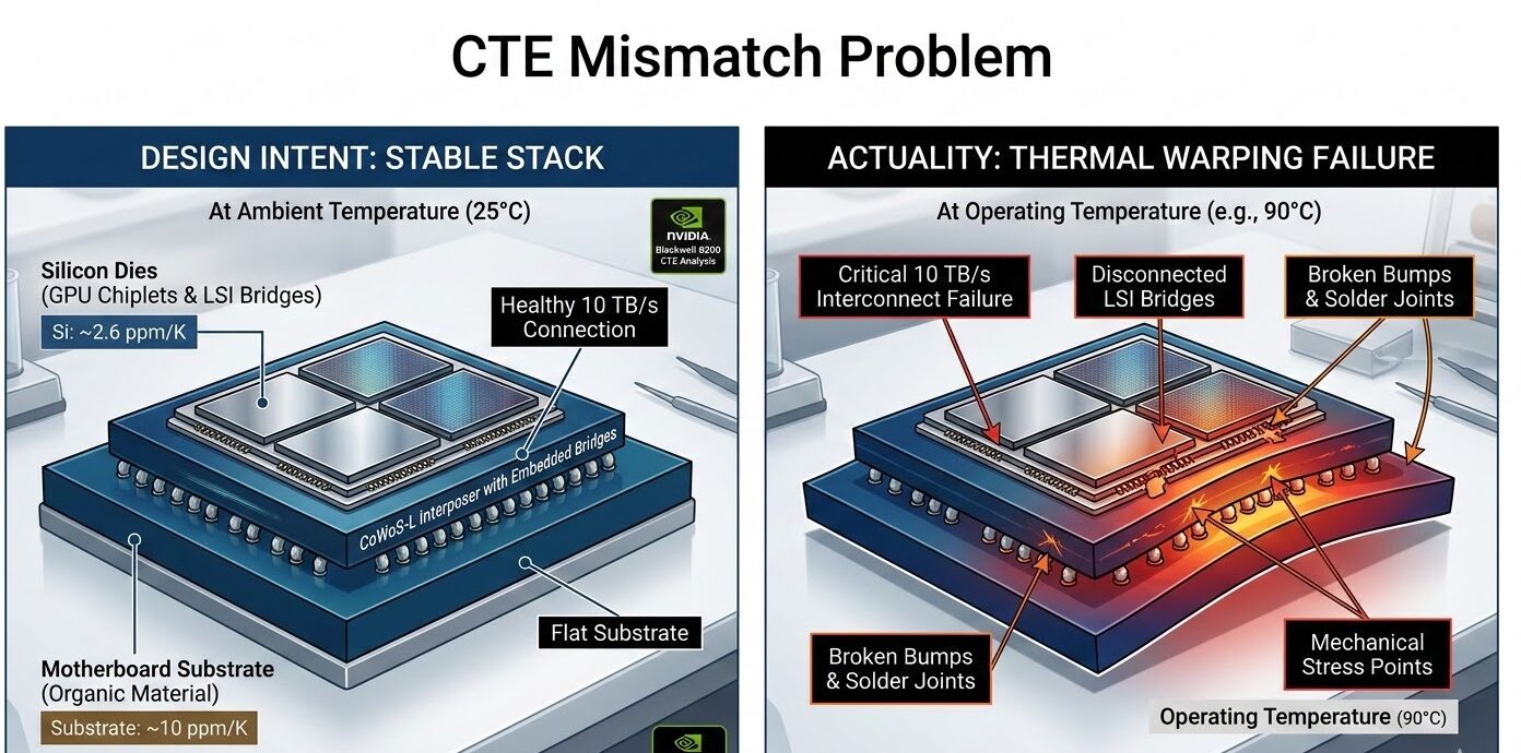
The Technical Reality: CoWoS-L and the CTE Mismatch Problem
Understanding the Packaging Revolution
To grasp why Blackwell stumbled, you need to understand what makes it different from its predecessor, Hopper. While the H100 used TSMC’s CoWoS-S (Chip-on-Wafer-on-Substrate with Silicon interposer) packaging, Blackwell introduced CoWoS-L a technology that replaces the monolithic silicon interposer with a redistribution layer (RDL) interposer equipped with local silicon interconnect (LSI) bridges.
This change wasn’t arbitrary. CoWoS-L allows for building systems-in-package up to six times the reticle size, enabling NVIDIA to create the massive GB200 “superchip” that combines two B200 GPUs with a Grace CPU. The technology promises better yields by avoiding the limitations of large silicon interposers.
But here’s the catch: CoWoS-L had never been used at this scale before.
The Coefficient of Thermal Expansion (CTE) Nightmare
The root cause of Blackwell’s delay was a mismatch in the Coefficient of Thermal Expansion (CTE) between different materials in the package.
Here’s what that means in plain English:
When materials heat up, they expand. When they cool down, they contract. The problem arises when different materials expand at different rates. In Blackwell’s case, the package contained:
Silicon has a CTE of approximately 2.6 ppm/K, while organic substrates expand at around 10 ppm/K.
When these components heat up during operation especially in dense server configurations they expand at different rates, causing mechanical stress that leads to warping and eventual system failure.
This wasn’t a minor issue. The LSI bridges between the two main compute dies are critical for maintaining the 10 TB/s chip-to-chip interconnect. Any misalignment breaks the connection,
The Mask Redesign: Why Three Months?
When the CTE mismatch was discovered, NVIDIA had to redesign the top metal layers and bumps of the GPU silicon. This required new photomasks the templates used in lithography to pattern each layer of the chip.
Creating new masks isn’t trivial. At the 4nm process node Blackwell uses, EUV (Extreme Ultraviolet) lithography involves complex computational physics to account for diffraction effects and optical distortion. TSMC actually uses NVIDIA’s own supercomputers to perform “computational lithography” for mask optimization.
Each new mask set takes approximately three months to design, verify, and qualify including identifying the problem, implementing fixes, and producing test wafers.
NVIDIA had to iterate through this process while maintaining the functional design of the chip unchanged.
The Overheating Saga: A Separate but Related Crisis
Server Rack Design Failures
While the CTE issue was being resolved, another problem emerged: overheating in server racks.The GB200 NVL72 system—a full rack solution containing 72 Blackwell GPUs—was experiencing thermal issues when GPUs were connected at scale.Unlike the CTE problem, which was a chip-level packaging issue, this was a system-level thermal management challenge.
The Information reported that NVIDIA had to redesign the server racks multiple times, with each iteration aimed at solving heat dissipation in densely packed configurations.The racks, designed to connect up to 72 GPUs simultaneously, were generating more heat than anticipated, potentially damaging neighboring components.
Liquid Cooling Complications
Blackwell represents NVIDIA’s push toward liquid cooling for high-density AI systems. The GB200 NVL72 uses direct liquid cooling (DLC) to handle the 120kW power draw per rack.
However, early deployments faced issues with:
By early 2025, suppliers including Foxconn, Inventec, Dell, and Wistron reported solving these issues through “a series of breakthroughs,” allowing production to ramp up.
The Business Impact: Who Got Hurt (And Who Didn’t)
The Hyperscaler Dilemma
The delay’s impact varied significantly by customer:
Microsoft: Had planned to deliver 55,000-65,000 GB200 GPUs to OpenAI by Q1 2025. This timeline became unachievable.
Google: Had ordered over 400,000 GB200 chips in a deal exceeding $10 billion. Despite having its own TPUs, Google was betting heavily on Blackwell for specific workloads.
Meta: Also placed approximately $10 billion in orders, needing the hardware for AI infrastructure expansion.
Amazon: Had shifted orders from Hopper to Blackwell, leaving them in a particularly difficult position during the delay.
NVIDIA’s Strategic Response
Rather than leaving customers empty-handed, NVIDIA executed a clever product segmentation strategy:
-
Extended Hopper Lifespan: The H100 and H200 remained in production to fill the gap, with demand actually increasing as customers sought available alternatives.
-
B200A Introduction: A new “air-cooled” variant using CoWoS-S packaging instead of CoWoS-L, targeting lower-to-mid-range AI systems. This used the same die as the China-compliant B20 chip.
-
Prioritized GB200: NVIDIA focused limited CoWoS-L capacity on the high-margin GB200 NVL72 systems rather than individual B100/B200 GPUs.
This approach protected NVIDIA’s revenue while managing the manufacturing constraints.
Jensen Huang’s Mea Culpa: Why “100% NVIDIA’s Fault” Matters
In October 2024, Jensen Huang made a statement that surprised many industry observers:
“We had a design flaw in Blackwell, it was functional, but the design flaw caused the yield to be low. It was 100% Nvidia’s fault.”
This admission was significant for several reasons:
1. Protecting the TSMC Relationship Initial reports had suggested TSMC’s CoWoS-L technology was to blame, potentially straining the three-decade partnership between the companies. Huang explicitly dismissed these reports as “fake news,” clarifying that TSMC had actually helped fix the issue quickly.
2. Managing Market Expectations By taking responsibility, NVIDIA controlled the narrative. The delay became a manageable engineering challenge rather than a fundamental architecture failure.
3. Technical Accuracy Huang’s statement was precise: the chip was “functional” but had yield issues. This distinction matters—Blackwell wasn’t broken; it just couldn’t be manufactured economically at scale.
The Yield Reality: What 90-95% Means
Supply chain sources revealed that B200 chips were achieving yields between 90-95% below TSMC’s internal standards.In semiconductor manufacturing, yield is everything. A 95% yield sounds good, but when you’re producing millions of chips, that 5% defect rate represents enormous cost. For a chip as complex as Blackwell with two reticle-sized dies, 192GB of HBM3e memory, and a sophisticated packaging scheme every percentage point of yield matters.
The CTE mismatch meant some percentage of chips would pass initial testing but fail after thermal cycling in real-world deployment. This is the worst kind of defect: the “time bomb” that appears only after customers install the hardware.
Why This Delay Was Actually Inevitable
The “Move Fast and Break Things” Problem
NVIDIA has delivered the most aggressive product roadmap in semiconductor history. Blackwell moved to a new architecture, new packaging technology, new cooling solutions, and new system-level integration simultaneously.As one analyst noted, this isn’t strictly a “design flaw” in the traditional sense it’s the consequence of “testing the upper limits of manufacturing complexities”.
The CoWoS-L Transition
TSMC’s shift from CoWoS-S to CoWoS-L represents a fundamental packaging technology transition. While CoWoS-S uses a monolithic silicon interposer (limited by reticle size), CoWoS-L uses multiple silicon bridges embedded in an organic interposer.This transition was always going to have teething problems. NVIDIA was simply the first to attempt CoWoS-L at this scale.
The Reticle Limit Problem
Modern AI chips are pushing against the physical limits of lithography. The reticle limit the maximum size a single chip can be is forcing companies toward chiplet architectures and advanced packaging. Blackwell’s dual-die design with high-bandwidth interconnect is the future, but the manufacturing infrastructure is still catching up.
The Road Ahead: Where Blackwell Stands Now
As of early 2026, Blackwell has moved past its initial struggles:
The delay, while painful, appears to have been successfully navigated without long-term damage to NVIDIA’s market position.
Lessons for the AI Hardware Industry
1. Packaging Is the New Battleground
As transistor scaling slows, advanced packaging becomes the primary driver of performance gains. But packaging complexity introduces new failure modes that the industry is still learning to manage.
2. Thermal Management Is Critical
AI chips are power-hungry, and power generates heat. The move to liquid cooling and dense server configurations requires rethinking thermal design at every level from individual dies to full data centers.
3. Yield Management Requires Transparency
NVIDIA’s handling of the delay particularly Huang’s direct acknowledgment demonstrates that transparency about manufacturing challenges can maintain trust even when products are delayed.
4. The Chiplet Transition Won’t Be Smooth
The industry’s move toward chiplet-based designs and advanced packaging will encounter similar challenges. Companies should expect and plan for teething problems when adopting new packaging technologies.
Conclusion: A Bump in the Road, Not a Derailment
The Blackwell delay was significant three months in an industry where three weeks can mean the difference between market leadership and playing catch-up. But it wasn’t catastrophic.
The fundamental architecture was sound. The CTE mismatch was a manufacturing optimization problem, not a design failure. And NVIDIA’s response taking responsibility, maintaining customer relationships, and managing the transition demonstrates the maturity of a company that has learned to navigate the complexities of leading-edge semiconductor manufacturing.
For the AI industry, the delay was a reminder that hardware progress isn’t always linear. The companies building the infrastructure for the AI revolution are pushing against physical limits, and sometimes those limits push back.
But Blackwell is here now. And if NVIDIA’s history is any guide, the next generation will face its own challenges and overcome them too.
FAQ: NVIDIA Blackwell Delay
Q: Was Blackwell delayed due to TSMC’s manufacturing problems?
A: No. Jensen Huang explicitly stated the design flaw was “100% NVIDIA’s fault,” though TSMC’s CoWoS-L packaging technology was new and contributed to the complexity.
Q: Did the delay affect NVIDIA’s stock price?
A: The stock experienced volatility in August 2024 when delays were announced, but recovered as the company demonstrated effective management of the situation.
Q: Are Blackwell GPUs available now?
A: Yes. Mass production began in late 2024, with full ramp-up through 2025. The initial design issues have been resolved.
Q: How does this compare to Intel’s Sapphire Rapids delays?
A: Intel’s Sapphire Rapids reportedly had around 500 bugs requiring a dozen steppings. NVIDIA’s Blackwell issue was resolved with a single mask change, making the fix relatively quick by comparison.
Q: Will this delay affect NVIDIA’s competitive position?
A: Unlikely. AMD and Intel face similar manufacturing challenges, and NVIDIA’s Hopper generation remained available to fill the gap. No competitor was positioned to capitalize on the delay.
Related Articles:
This article represents independent analysis based on publicly available information and industry reports. All technical details have been cross-referenced with multiple sources to ensure accuracy.